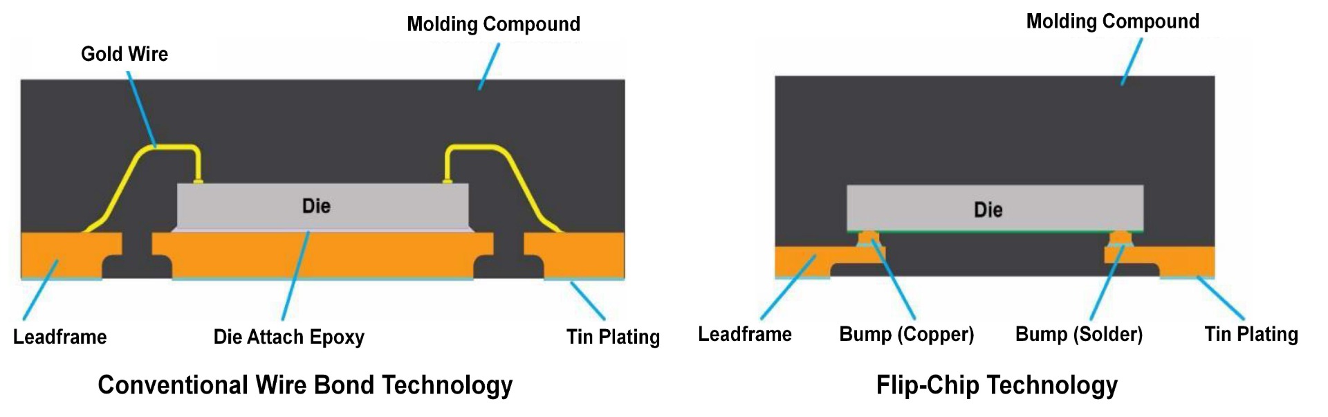
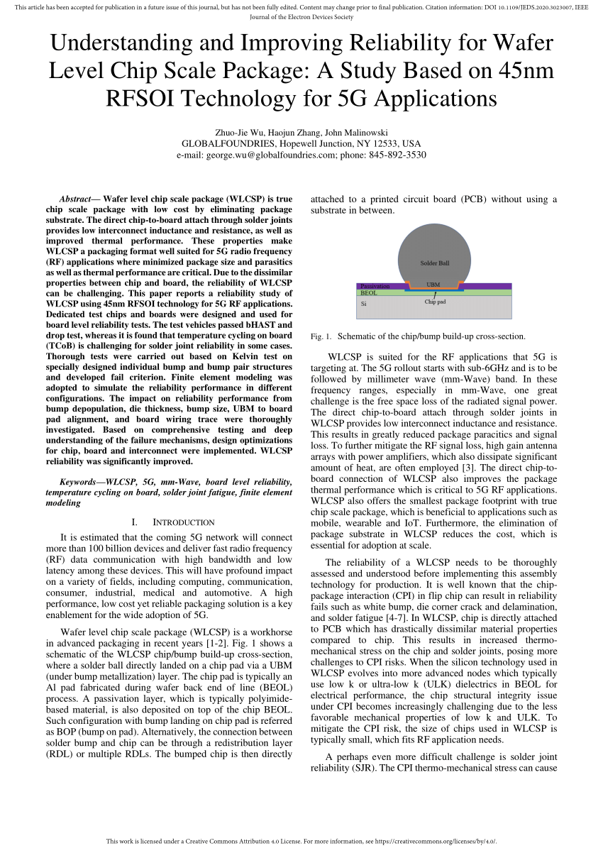
Schematic of the chip/bump build-up cross-section.

Cross-section of solder microbump on the Si chip (not in scale) (a

Challenges Grow For Creating Smaller Bumps For Flip Chips

PDF) Understanding and Improving Reliability for Wafer Level Chip
IC Substrate - Basic Introduction to Integrated Chip Substrate
Microscopy Solutions for Advanced Semiconductor Packaging

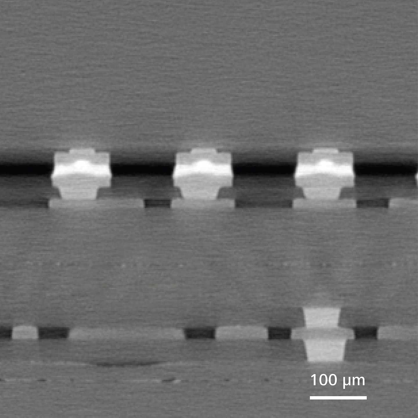
SEM image of a cross section of an unstressed 30 μm solder bump
Predicting the VDS Switching Spike with the Parasitic Inductance
Introduction (Chapter 1) - Wireless Interface Technologies for 3D

Hybrid Bonding Process Flow - Advanced Packaging Part 5
Package Substrate, SAMSUNG ELECTRO-MECHANICS
PDF) Understanding and Improving Reliability for Wafer Level Chip

High-lead flip chip bump cracking on the thin organic substrate in

Effects of build-up printed circuit board thickness on the solder