App note: Exposed pads on some IC packages – Dangerous Prototypes
By A Mystery Man Writer

Open-Source Method Makes Possible Two-Layer PCBs With Through-Plating At Home

Bus Pirate - DP
The Ultimate PCB Design Software Comparison

Dangerous Prototypes – Page 534 – Open source hardware projects
TIP #014: If you have an exposed pad on your component, consider

Design World/EE Network - Power Electronics Handbook by WTWH Media
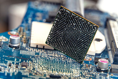
How to Correctly Understand The Ball Grid Array Soldering Technology

How to desolder QFP chips with a normal soldering iron : r/electronics
Open-Source Method Makes Possible Two-Layer PCBs With Through

Soldering ICs with Exposed DAP — Neurochrome

PCB Resistors Applications- Circuit Control Through Resistance
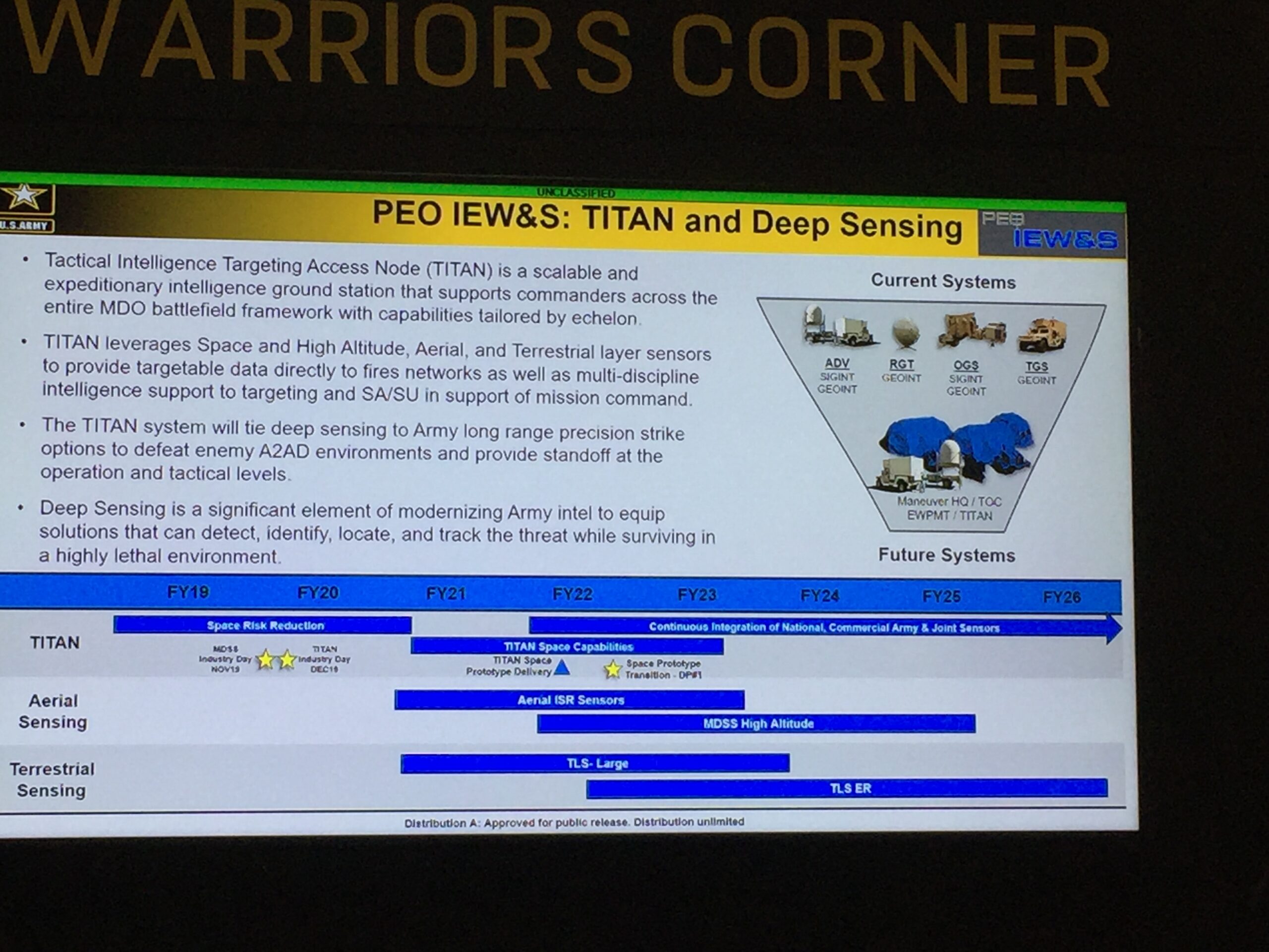
Army's TITAN Ground Station To Link Multi-Domain Sensors to Shooters - Breaking Defense


)