pcb - What is the pad size required for this BGA AW H3 Chip? - Electrical Engineering Stack Exchange

I'm trying to figure out the pad size to use for my footprint according to this datasheet.The last page in the datasheet has the package dimensions. I've also posted the relevant information in a p
2 x 3 Perfboard, Electronics Prototyping
How to Create a SMD pad using the Allegro Padstack Editor? - PCB Design Tutorial - PCBway

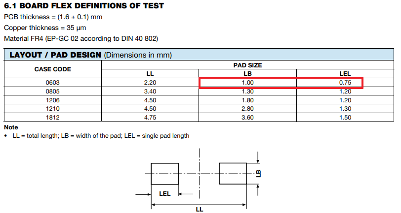
pcb design - I have a doubt on taking pad dimensions in this below picture what is the pad width and height.any body kindly clear my doubt - Electrical Engineering Stack Exchange

pcb design - Recommended Pad Layout Hole Size - Electrical Engineering Stack Exchange

What should be paid attention to in SMT patch processing BGA
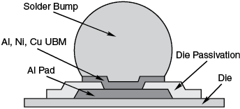
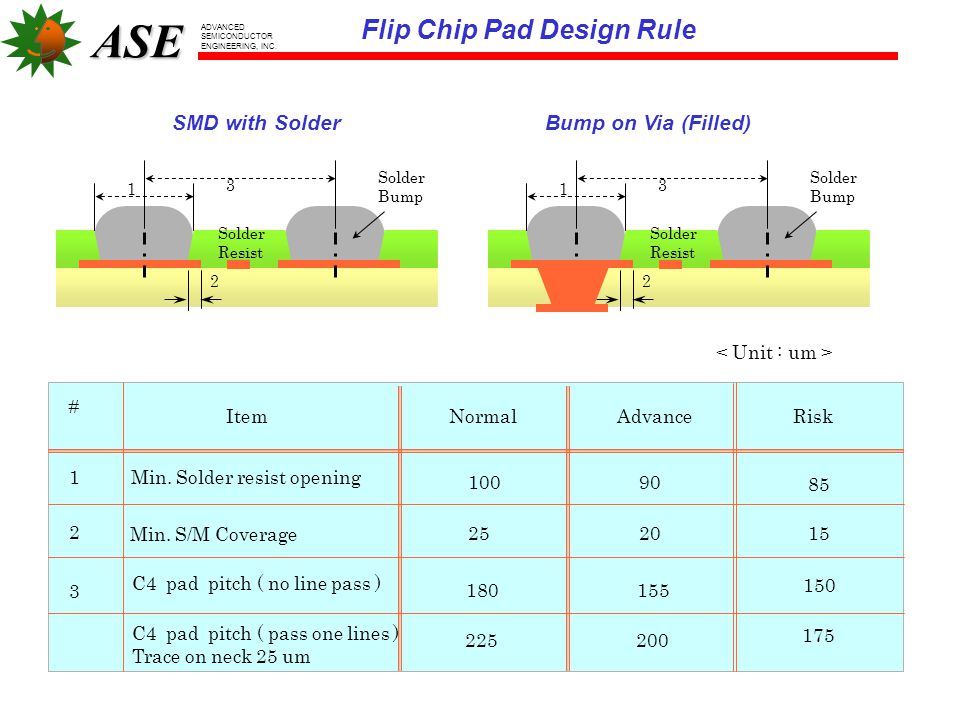
PCB Pad Size Guidelines: Finding the Proper Pad Sizes for Your Circuit Design

BGA Pad Size Deep Dive Component Creation
PCB SMT Factory China,X-RAY Inspection BGA Assembly IC Programming One-stop PCB Assembly

Energies June-2 2020 - Browse Articles
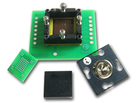
BGA Sockets - Ironwood Electronics
2 x 3 Perfboard, Electronics Prototyping
Working With BGAs: Design And Layout