Balancing Layers in Your PCB Layout
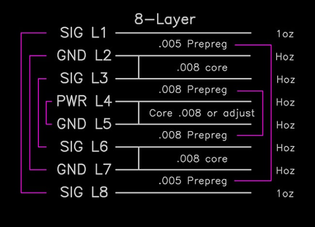
Balancing layers in your PCB layout stack-up, which both layer surfaces and cross-sectional structure of the circuit board are reasonably symmetrical.
Circuit Board 4-Layer PCB Stackup Planning, Advanced PCB Design Blog

PCB Layers Explained: Everything You Need to Know
Best Guide To PCB Traces: Width, Thickness And Design Fix Recommendations - Jhdpcb
Epec's Blog
Defining the Layer Stack in Altium Designer Altium Designer 24 Technical Documentation

TT12 PCB Metalization Basics, PDF, Printed Circuit Board
How to Design and Fabricate the Best 4 Layer PCB Stackup with

How To Create PCB For Drone - PCB Design Tutorial - PCBway

Understanding PCB Thickness: A Comprehensive Guide

Key Factors Influencing PCB Layer Stack Selection for Cost-Effective and High-Quality Designs
How to Design a PCB Layout - Circuit Basics

The Most Common 2-Layer PCB Design Mistakes and How To Avoid Them
PCB Layer stack-up

Trace PCB: A Comprehensive Guide